The Apple A19 SoC has arrived as a technological marvel within the highly anticipated iPhone 17, setting new standards in mobile processing. This advanced SoC showcases Apple’s unparalleled semiconductor technology, crafted with precision using the revolutionary 3nm process technology. Featuring an enhanced A19 chip, the device not only promises superior performance but also remarkably improved energy efficiency compared to its predecessors. In addition, the intricate A19 die shot reveals a sophisticated architecture designed for optimal multitasking and high-fidelity graphics, further appealing to tech enthusiasts. As the landscape of mobile computing continues to evolve, the Apple A19 SoC stands at the forefront, propelling innovation in the smartphone market.
Unveiling the next generation of mobile processors, the A19 chip marks a significant leap in the realm of smartphone technology with its inclusion in Apple’s iPhone 17. This cutting-edge system-on-chip (SoC) integrates multiple advancements tailored for peak operational efficiency and high-performance computing. Utilizing a state-of-the-art 3nm manufacturing process, the A19 is engineered to enhance both graphics capabilities and artificial intelligence operations within mobile devices. The impressive die shot of this powerhouse chip highlights its dense architecture and optimized layout, a testament to Apple’s dedication to continual improvement in semiconductor design. By pushing the boundaries of processing power, the iPhone 17 encapsulates the future of mobile technology.
Unveiling the Apple A19 SoC: A Comprehensive Overview
The Apple A19 SoC, launched with the iPhone 17 in September 2025, marks a significant leap in semiconductor technology. Utilizing TSMC’s cutting-edge 3nm process technology, the A19 chip exhibits a remarkable increase in transistor density compared to its predecessor, the A18 chip. This transition to third-generation technology not only enhances performance but also bolsters energy efficiency, making the A19 a standout in the world of high-end mobile processing. As smartphone demands grow, such advancements in chip design ensure that Apple remains at the forefront of innovation.
In the realm of mobile processors, the Apple A19 SoC exhibits a finely-tuned hybrid architecture that optimizes performance by balancing efficiency and power. This structure integrates performance cores for demanding tasks while employing efficiency cores for everyday activities, a hallmark of Apple’s approach to semiconductor design. Moreover, this new chip architecture is paired with an array of upgraded features, including advancements in the GPU that support larger models of the iPhone 17, ready to tackle high-performance gaming and AI-driven applications seamlessly.
Deep Dive into Apple A19 Chip Technology
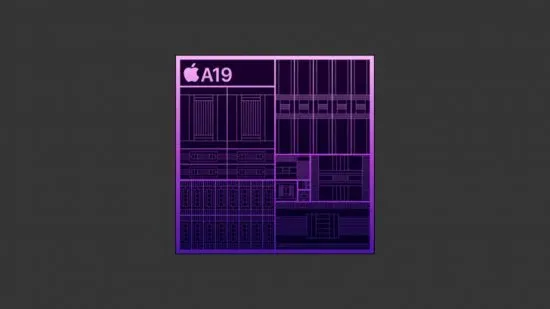
Analysts and tech enthusiasts are particularly excited about the detailed die shots of the Apple A19 chip, which offer profound insights into its design and functionality. High-resolution floorplan images reveal the complex arrangement of logic blocks, cache banks, and interconnects that keep the SoC functioning optimally. Each component is meticulously engineered to ensure that the A19 chip operates efficiently under various loads, highlighting the sophistication of Apple’s semiconductor technology. This level of detail emphasizes how Apple’s design philosophy prioritizes not just performance but also thermal management and power consumption.
Furthermore, the A19 die shot analysis showcases Apple’s relentless pursuit of refinement in its semiconductor technology. Every aspect, from the layout to the interconnect pathways, reflects years of research and development. The improvements seen in the Apple A19 SoC, particularly its image signal processor and neural engine, are pivotal for enhancing on-device capabilities. With more demanding image processing and artificial intelligence tasks being carried out on mobile devices, the upgrades to these components solidify Apple’s leadership in creating powerful and efficient SoCs.
Performance and efficiency enhancements are complemented by Apple’s strategic investment into the development of new features tailored specifically for the Pro variants of the iPhone 17. The success of the A19 chip further validates Apple’s roadmap for integrating advanced process technology into mainstream consumer devices, ensuring that users can expect not only seamless multitasking but also cutting-edge graphical experiences.
Understanding the 3nm Process Technology in the A19 SoC
At the core of the Apple A19 SoC’s advanced capabilities is its utilization of 3nm process technology, a revolutionary step forward in chip manufacturing. The transition from 5nm to 3nm allows for greater transistor density, which translates into improved processing power and efficiency. This small node size enables Apple to pack more functionalities into a compact space without increasing the chip size, allowing for not just improved performance but also enhancements in energy consumption, which is crucial for mobile devices.
With the A19 chip, Apple leverages the inherent advantages of the 3nm process, enabling it to deliver not only faster CPUs and GPUs but also improved thermal management capabilities. This is particularly beneficial in prolonging battery life, an essential factor for users who demand high performance from their devices without sacrificing uptime. The advancements made possible through this cutting-edge manufacturing process underline Apple’s commitment to pushing the boundaries of what’s possible with semiconductor technology.
The Architecture of the Apple A19 Die
The architecture of the Apple A19 die is a study in efficiency and complexity, combining various elements into a cohesive package. The die layout reveals a sophisticated arrangement of cores, cache, and interfaces that underpin the chip’s functionality. This architectural refinement means that while the A19 serves as the powerhouse for the iPhone 17, it also does so within a surprisingly compact footprint, allowing for more innovative designs in mobile device manufacturing.
Examining the A19 die further unveils the integration of a powerful image signal processor and enhanced GPU capabilities specifically designed for the professional-grade models of the iPhone 17. These upgrades not only enhance device performance in gaming and high-resolution content creation but also elevate user experiences in photography and videography. Apple’s design choices reflect a deep understanding of user needs and the future landscape of mobile technology.
AI and Power Management Innovations in the A19
A key area of innovation within the Apple A19 SoC is its enhanced Neural Engine, designed to support the growing demand for on-device artificial intelligence (AI) capabilities. With upgrades that enable faster machine learning tasks, the A19 chip can handle advanced computational photography, augmented reality, and real-time video processing with ease. This level of performance not only enhances user experiences but also sets a new standard for AI integration in smartphones.
In addition to AI enhancements, the Apple A19 chip also features advanced power management components, allowing users to enjoy peak performance without compromising battery life. By allocating resources intelligently and adjusting power usage based on activity levels, the A19 ensures that the iPhone 17 remains efficient during resource-intensive tasks. This careful balance of power and performance speaks to Apple’s dedication to user-centric design in its semiconductor technology.
Comparing Apple A19 with Previous Generations
The Apple A19 represents a significant upgrade over its predecessors, particularly the A18 series which utilized TSMC’s 5nm process. When comparing the two, the differences in performance and efficiency are striking. The A19’s architectural enhancements lead to noticeable improvements in computational tasks, graphics rendering, and overall system responsiveness, providing a quantum leap for users looking for the latest in mobile technology.
Moreover, while the A18 was a powerful chip, the transition to the 3nm process for the A19 has introduced advanced thermal and power management features, allowing for sustained high-performance levels without overheating or excessive battery drain. This has made the iPhone 17 not only faster but also more capable of handling intensive applications like gaming and high-resolution video editing, reinforcing Apple’s reputation for creating top-tier mobile devices.
The Future of Apple Semiconductor Technology
As we look to the future, the Apple A19 SoC sets a high bar for subsequent generations of chip technology. With Apple’s ongoing investment in R&D, we can anticipate continued advancements in performance, efficiency, and integration of AI capabilities into upcoming models. The A19 is more than just a powerful chip; it is a signpost indicating where Apple intends to go in the realm of semiconductor innovation.
In conclusion, the Apple A19 not only solidifies Apple’s role as a leader in the semiconductor industry but also reflects a broader trend towards smaller, more powerful chips derived from advanced manufacturing processes. With each generation, Apple continues to push the boundaries, ensuring that its devices are not only competitive in specs but also aligned with the future demands of consumer technology.
Insights from Apple A19 Die Shot Analysis
The die shot analysis of the Apple A19 chip provides invaluable insights into the engineering marvels of modern semiconductor technology. By examining these high-resolution images, analysts can glean essential information on the internal structures and technologies that contribute to the chip’s performance. The intricate designs visible in the die shots highlight the advanced manufacturing processes, such as the use of multi-layer structures that enhance performance while reducing power consumption.
Additionally, the analysis allows manufacturers and competitors to understand Apple’s strategic choices in semiconductor design, potentially influencing future chip development across the industry. As other companies strive to keep pace with Apple’s innovations, the insights gained from the A19 die shot may inspire new approaches and lead to further breakthroughs in the semiconductor realm.
Key Components of the Apple A19 Architecture
At its core, the Apple A19 architecture is composed of several key components that work collaboratively to deliver exceptional performance. This includes a series of high-performance CPU cores designed for handling rigorous tasks, complemented by efficiency cores that manage lighter, everyday applications. The separation of components allows for dynamic resource allocation, ensuring that the device operates smoothly across a range of usage scenarios.
Beyond the CPU, the integration of advanced GPUs specifically in the Pro models showcases Apple’s focus on high-performance graphics capabilities. With the A19, the graphical power available for mobile devices reaches new heights, facilitating immersive gaming and smooth content playback, reaffirming Apple’s dedication to providing users with unparalleled multimedia experiences.
Frequently Asked Questions
What are the key features of the Apple A19 SoC?
The Apple A19 SoC, powering the iPhone 17, boasts significant enhancements over its predecessor, utilizing TSMC’s advanced 3nm process technology. It features a hybrid core architecture that combines performance and efficiency cores, improved GPU performance with additional cores for Pro models, and upgraded components such as the image signal processor and Neural Engine, enhancing AI capabilities and imaging performance.
How does the Apple A19 chip improve energy efficiency?
The Apple A19 chip achieves enhanced energy efficiency through its innovative 3nm process technology, which allows for higher transistor density while reducing power consumption. This advancement enables devices like the iPhone 17 to provide better performance without sacrificing battery life, making it more sustainable for users.
What performance improvements can I expect from the A19 die shot analysis?
Analysis of the A19 die shot reveals modest performance improvements over the previous A18 series, attributed to its advanced architecture and core enhancements. The integration of more GPU cores specifically designed for Pro models also contributes to better graphics performance, especially in demanding applications.
What is the significance of the A19 die shot in understanding Apple’s semiconductor technology?
The A19 die shot is significant as it visually represents Apple’s ongoing advancements in semiconductor technology. It highlights the chip’s complex layout, including logic blocks and interconnects, while showcasing Apple’s commitment to enhancing manufacturing processes, particularly with its adoption of 3nm technology.
How does the hybrid architecture of the Apple A19 SoC benefit users?
The hybrid architecture of the Apple A19 SoC combines performance and efficiency cores, allowing the iPhone 17 to optimize tasks by allocating resources based on the demands of applications. This results in faster processing times for intensive tasks while conserving battery life during less demanding activities.
What upgrades are included in the Apple A19 chip for enhanced AI capabilities?
The Apple A19 chip includes significant upgrades to its Neural Engine, enabling advanced on-device AI processing. These enhancements facilitate faster and more efficient machine learning tasks, improving features such as image recognition, real-time processing, and overall responsiveness in AI-driven applications.
Where can I view high-resolution images of the Apple A19 SoC?
High-resolution die shot images of the Apple A19 SoC are available for viewing. These images showcase both the frontside and backside layouts, providing detailed insights into the design and architecture of the chip, which are essential for understanding its functionalities and technological advancements.
| Project Name | Device | Category | Project Year | Process Node | Core Architecture | GPU Enhancements | Key Upgrades |
|---|---|---|---|---|---|---|---|
| Apple A19 SoC | iPhone 17 | Teardown Die Shot | September 2025 | TSMC 3 nm (N3P) | Hybrid (performance + efficiency cores) | Additional cores for Pro models | Image signal processor, display engine, and Neural Engine upgrades |
Summary
The Apple A19 SoC marks a significant advancement in semiconductor technology, revealing improvements in performance and efficiency. Built on TSMC’s third-generation 3 nm process, this chip optimizes the capabilities of the iPhone 17 and enhances on-device AI functions. With its hybrid core architecture and GPU enhancements, the A19 SoC not only caters to general performance demands but also supports the growing requirements of advanced mobile applications. Overall, the A19 represents Apple’s commitment to pushing technological boundaries in the smartphone industry.